PCB Design & Layout
About Our Board Designs
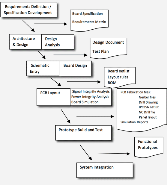
Whether your project is a new design or a design refresh due to parts obsolescence or feature improvements, the Integre team brings the expertise to deliver your project on-schedule and on-budget. Integre’s services cover the complete design flow from requirements through manufacture and test.
Integre is available to help accelerate one specific design step, such as logic design, schematic entry, or layout, to providing end to end product development from requirements to delivery of completed assemblies ready for integration into your system.
Design Flow and Deliverables

Integre PCB Designs


Processes and tools used to design printed circuit boards vary from company to company. Variations of design flows are too numerous to list but typically involve all or some of the following:
Design And Architecture Specification
- HW architecture description
- Cost analysis
- Interface and bandwidth definitions
- SW programming sequences
- EMI design practices
Design Entry
- Graphical design entry from company libraries
- Symbol and part number generation if necessary
- Simulatable vhdl or verilog netlist generation
- Netlist generation
- Parts list generation
Simulation Philosophy (Full, Partial, None)
- Timing analysis
- Functional rtl and gates (min, typ, max) for fpga’s
- Timing models (min, typ, max) for glue logic from company libraries (or download: memories for instance)
- Test writing, self checking environment
- Post layout signal integrity analysis
Mechanical
- Board shape and connector placement to support proper electrical design and manufacturability
- System level faraday enclosures
Prototype Manufacturing
- Design for test issues (bed of nails, jtag, etc)
- Interaction with layout house (or on site), oversee layout
- Interaction with board assembly house
Integration Support
- Debug with the SW team
- EMI testing
- Thermal testing
- High reliability mixed digital and analog subsystem design
- System architecture analysis and specification development
- Advocating logic, hardware, and software co-design
- Communications and control applications leveraging FPGA logic
- Design for fault isolation and diagnostic visibility
- Design using worst case and failure modes and effects analysis
- Layout specifications for EMC and reduced EMI
- Circuit Board Design and Layout:
- Built for test ASIC/FPGA evaluation circuit board design
- Reference design and breadboard circuit boards
- Layout specifications for EMC and reduced EMI
What They Say
![]() We have run through the dynamic testing of the board under load and I am happy to report that the board provided the outputs that we were looking for.
We have run through the dynamic testing of the board under load and I am happy to report that the board provided the outputs that we were looking for. ![]()
– Technical Lead, Power Semiconductor Company
